The question comes up in every technical evaluation: why can't we just run CRYSTALS-Kyber as a software library on our existing authorization servers? The answer is not that software implementations don't work — they do, and they pass NIST's test vectors. The answer is that wire-speed key generation for financial transaction infrastructure requires computational characteristics that general-purpose CPUs cannot provide at production transaction volumes, and that the physical security properties of key operations in regulated environments require hardware isolation that a software process cannot replicate.
This article examines the computational architecture of CRYSTALS-Kyber, specifically the Number Theoretic Transform that is the core bottleneck, and explains why FPGA implementation changes the performance and security picture fundamentally — not incrementally.
The computational core of Kyber: polynomial multiplication via NTT
CRYSTALS-Kyber's security derives from the difficulty of solving Module-LWE problems in polynomial rings. Specifically, the ring Z_q[x]/(x^n + 1) where n=256 and q=3329. All key operations — key generation, encapsulation, and decapsulation — reduce to matrix-vector multiplications over this ring, where each element is a degree-255 polynomial with coefficients in Z_3329.
Naive polynomial multiplication of two degree-255 polynomials requires O(n^2) = 65,536 multiplications and additions. For Kyber-1024 with its k=4 module dimension, a single matrix-vector multiplication involves 16 such polynomial products. This is computationally intractable at wire speed without algorithmic acceleration.
The Number Theoretic Transform (NTT) reduces this to O(n log n) operations by converting polynomials to their NTT representation, performing pointwise multiplication (O(n)), and inverting. For n=256, NTT requires 256 * log_2(256) / 2 = 1,024 butterfly operations, each involving a modular multiplication and addition. The total operation count for a Kyber-1024 encapsulation is on the order of 50,000–80,000 modular operations, depending on the specific implementation.
Why CPUs struggle with NTT at payment scale
Modern x86-64 processors handle NTT reasonably well for isolated cryptographic operations — the AVX2 instruction set supports vectorized modular arithmetic that allows 16-way parallelism for 16-bit operations. Reference implementations using AVX2 achieve approximately 15,000–22,000 Kyber-1024 operations per second on a single core at ~3.5 GHz.
At first glance, 20,000 ops/sec per core seems adequate. A dual-socket server with 64 cores could theoretically sustain 1.28 million ops/sec. But this analysis breaks down in three ways for payment authorization environments:
1. The cores are not available
Authorization servers are not idle machines waiting to run cryptography. They run authorization application logic, database clients, fraud detection models, routing logic, and protocol handling simultaneously. A server sized for 2,500 authorization transactions per second might use 60–70% of CPU capacity on application logic at peak load, leaving 10–15 cores free for cryptographic operations — not 64.
2. Shared cache contention degrades NTT performance
NTT butterfly operations have a specific memory access pattern: the 256-element polynomial must be traversed in bit-reversed order across log_2(256) = 8 stages. This produces irregular memory access patterns that do not cache-line-align predictably. When application code and NTT operations compete for the same L3 cache on a shared socket, effective NTT throughput drops 15–30% from single-threaded peak.
3. P99 latency degrades non-linearly under burst
At 80% CPU utilization, the average throughput may appear adequate. But at burst peaks — authorization spikes during retail hours, end-of-day settlement batches, holiday transaction volumes — utilization hits 95–99% and the scheduler queue causes P99 latencies to spike to 5–20x median. For authorization flows with 200ms total round-trip budgets, this turns a 2ms cryptographic operation into an 18ms one unpredictably.
THE BURST PROBLEM
Payment authorization traffic is not uniformly distributed. Black Friday traffic can be 8–12x typical daily average for the same infrastructure. Software PQC on general-purpose servers must be sized for peak burst, not average load. Hardware offload eliminates this over-provisioning requirement — CQ1 sustains >18K ops/sec continuously regardless of host server CPU load.
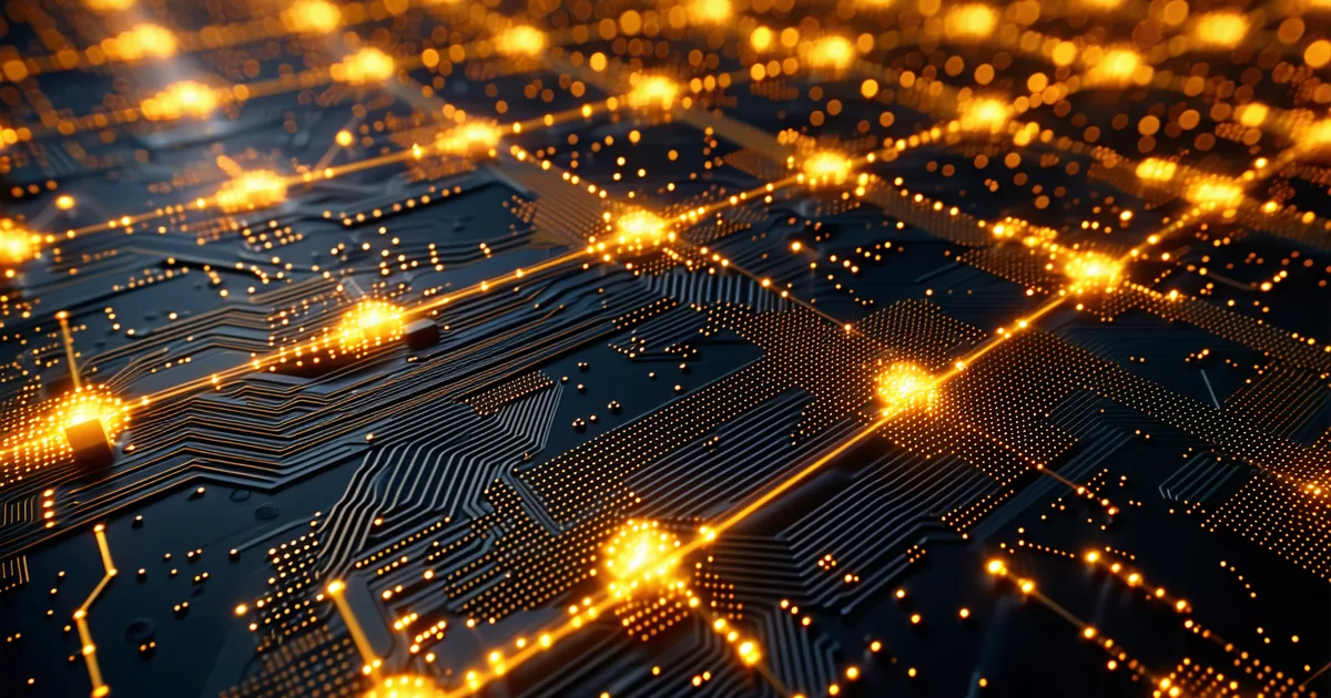
FPGA implementation: why the architecture changes the math
An FPGA implementation of the Kyber NTT does not execute the butterfly operations sequentially on a single arithmetic unit. It implements the butterfly network as physical logic — each butterfly stage is a separate parallel circuit operating simultaneously on a different subset of the polynomial elements.
For a 256-element NTT with 8 stages, an FPGA can instantiate all 8 butterfly layers as parallel hardware. Each layer processes 128 butterfly pairs simultaneously. With a 200 MHz clock and pipeline filling within a few cycles, the effective throughput is determined by the pipeline depth and clock rate, not by sequential operation count.
The practical result: an NTT on 256 elements that takes ~400 clock cycles sequentially on an AVX2-optimized CPU (at 3.5 GHz, ~114ns) can be implemented in an FPGA pipeline with a latency of 20–30 clock cycles at 200 MHz (~100–150ns) but with full throughput at every clock cycle after the pipeline fills. When processing a continuous stream of Kyber operations, the FPGA pipeline never stalls — each clock cycle produces one output, yielding a sustained throughput that scales with clock rate and parallel pipeline instances, not with sequential operation count.
CQ1's NTT pipeline architecture
CQ1 implements Kyber-1024 NTT in a pipelined FPGA fabric with the following characteristics:
- Parallel NTT instances: Multiple independent NTT pipelines operating concurrently, each handling a separate Kyber operation. Operations are dispatched round-robin across pipelines.
- On-fabric polynomial memory: All 256-element polynomial arrays are stored in FPGA block RAM with single-cycle access. No external DRAM access during NTT execution — all operations occur within the FPGA fabric's local memory hierarchy.
- Dedicated modular arithmetic units: Custom modular multiplication circuits for Z_3329 arithmetic, implemented as dedicated DSP block chains with zero software overhead. The modulus 3329 = 2^12 - 2^8 + 1 is a special prime that admits efficient Montgomery reduction.
- Hash acceleration: SHA-3 (Keccak-f1600) and SHAKE-256 implemented as hardware state machines alongside the NTT pipeline. Kyber's use of hash functions for public key generation and pseudorandom sampling runs in parallel with arithmetic operations rather than sequentially.
The combined effect: CQ1 executes a complete Kyber-1024 encapsulation — key generation to encapsulated ciphertext — in under 55 microseconds at the hardware level. The PKCS#11 interface layer adds approximately 0.1–0.2ms of host round-trip overhead. Total P99 latency at sustained 10,000 ops/sec is under 0.8ms. This is deterministic — there is no garbage collection, no OS scheduler preemption, no cache miss variance. Every operation at any load level takes the same time as the first operation.
Determinism: why latency variance matters as much as average latency
Financial systems are designed around latency budgets, not latency averages. A payment authorization that takes 150ms on average but occasionally takes 800ms fails SLA requirements even if the 99th percentile is acceptable. The 99.9th percentile — P999 latency — is what matters for systems processing 10,000+ transactions per minute.
Software PQC running on a general-purpose OS has P999 latency contributions from:
- OS scheduler jitter (process preemption, context switching): adds 0.1–2ms at high system load
- TLB misses during NTT memory access: 10–100 microseconds per miss at cold-start
- L3 cache eviction under application load: degrades NTT performance by 15–30% with high variance
- NUMA effects on dual-socket systems: NTT execution on a remote NUMA node increases memory latency 2–3x
CQ1's FPGA pipeline has none of these variance sources. The NTT runs in a clock-driven hardware state machine with deterministic memory access patterns on fabric-local memory. P50, P99, and P999 latencies are within 10% of each other at any load level up to maximum throughput. For systems designers building payment authorization infrastructure with sub-millisecond SLAs, this predictability is as important as the raw throughput number.
The physical security boundary: why isolation matters for key operations
The performance case for hardware PQC is strong on its own. The security case is separate and, for regulated financial infrastructure, more important.
CRYSTALS-Kyber's secret key is the set of polynomial vectors s and the noise distribution parameters used during key generation. During decapsulation, the module re-encrypts the decapsulated plaintext and compares — a timing differential in this re-encryption step, caused by branch-prediction behavior or cache state, can leak information about s. This is not a theoretical concern — power analysis attacks against AVX2 Kyber implementations have been demonstrated in academic literature.
CQ1's FPGA execution eliminates this attack surface at the architectural level:
- No shared memory with host CPU during key operations. The secret polynomial s is stored in FPGA block RAM that is not accessible from the PCIe host interface during operation.
- Constant-time execution at the hardware level. FPGA logic operates on clock cycles, not branch-prediction trees. Every Kyber decapsulation executes the same sequence of gate operations regardless of the input value.
- Active power conditioning in the FPGA supply rail reduces differential power analysis (DPA) signal below measurable thresholds. The DPA signal from NTT operations is attenuated by the power supply filtering circuitry inside the cryptographic boundary.
- Tamper-detection mesh surrounding the entire FPGA fabric triggers zeroization of all key material within 100ms of physical access detection.
This is the reason CQ1 is designed for FIPS 140-3 Level 3 validation rather than Level 1 (software) or Level 2. Level 3 requires the physical attack resistance characteristics that protect key operations from the side-channel vectors that software implementations cannot address.
Conclusion: the right tool for the specific use case
Software PQC libraries are correct tools for many applications. Browser TLS, mobile application encryption, and internal tooling where performance requirements are modest and hardware key boundaries are not mandated — these are appropriate software PQC use cases.
Payment authorization HSMs, SWIFT gateway key management, PKI root CA operations, and PIN encryption key generation are not. These use cases require hardware isolation for regulatory compliance, physical tamper resistance for security assurance, and deterministic latency for operational reliability. Dedicated silicon — FPGA-based hardware with purpose-built NTT pipelines and physical security boundaries — is the correct tool for these use cases, and it is why wire-speed lattice cryptography belongs in a module like CQ1, not in a software library on a shared server.
The power and thermal envelope: why FPGA in 1U makes sense
A common question about FPGA-based HSMs is whether the power draw and thermal profile are compatible with data center deployment alongside existing server infrastructure. The NTT pipeline in CQ1 runs within a 1U chassis with a thermal design power (TDP) consistent with standard rack-mount hardware. FPGA fabric is inherently parallel, and the NTT pipeline's power consumption scales with the number of butterfly units instantiated and the clock rate — not with the complexity of the computation, because the circuit depth is fixed regardless of input values.
A general-purpose CPU handling the same 18,000 Kyber-1024 ops/sec workload would require 6–8 dedicated cores running at 3.5GHz with AVX2, drawing substantially more power per operation due to the general-purpose execution units, branch predictors, and memory hierarchy all consuming power even when not needed for the NTT computation. The FPGA implements only the required logic — no unused execution units, no speculative execution, no branch predictor tables. Power per operation is lower even as throughput is higher, because the implementation matches the workload architecture rather than adapting a general architecture to a specific workload.
For financial data centers with strict power allocation per cabinet, this matters. Replacing a classical HSM (handling RSA-2048 operations) with CQ1 (handling Kyber-1024 operations at 8–15x higher throughput) within the same power envelope is not just feasible — it is often favorable, because the FPGA's power scaling with utilization is more predictable than a CPU server's power profile under mixed workloads.
What "wire speed" means in the context of 100GbE payment infrastructure
The term "wire speed" in network cryptography refers to the ability to process data at the rate it arrives on the network interface without introducing additional latency queuing. For a 100 Gigabit Ethernet interface carrying TLS-protected payment flows, wire-speed encryption means processing each arriving frame's cryptographic operations before the next frame arrives — typically within a few microseconds per frame at 100GbE line rates.
For a payment network segment operating at 10GbE with 1,500-byte TLS records, a new session negotiation requires a Kyber-1024 encapsulation to establish the session key. At 10,000 new sessions per second, you have 100 microseconds per session for the key establishment operation. Software Kyber on a dedicated CPU core runs at approximately 50–80 microseconds per operation in isolation. Under concurrent load on a shared server, this extends to 150–300 microseconds. The hardware target is under 55 microseconds with full pipeline utilization — which is the condition where hardware-accelerated key exchange stays off the critical path even at 10GbE session establishment rates.
The "wire speed" framing is also relevant for inline encryption use cases — where the HSM sits inline on the data path rather than as an out-of-band key management appliance. Inline key establishment requires that the cryptographic module processes each new connection's key exchange faster than connections arrive. At scale financial network segments where session establishment rates exceed 5,000 new TLS connections per second, software crypto cannot maintain inline wire speed. Hardware pipeline implementations can.
Comparison with ASIC approaches: why FPGA is the right choice for this generation
ASIC (Application-Specific Integrated Circuit) implementations of NTT would achieve higher clock rates and lower power per operation than FPGA. An ASIC designed specifically for Kyber-1024 NTT butterfly computation could potentially reach 500 MHz+ clock rates with sub-0.1μs per operation latency. So why is CQ1 built on FPGA rather than custom ASIC?
The answer is algorithm risk. FIPS 203 and FIPS 204 were finalized in August 2024. The history of cryptographic standards is not without examples of algorithms that required parameter updates or modifications after deployment — not breaks of the mathematical hardness assumption, but specification issues, side-channel vulnerabilities discovered in specific implementations, or parameter refinements based on cryptanalytic progress. An ASIC implementation of Kyber-1024 that bakes the current parameter set into silicon cannot be updated if a parameter change is necessary. An FPGA implementation can receive firmware updates that modify the NTT parameter tables, polynomial modulus, or error distribution within the validated security boundary.
We are not saying ASIC is the wrong long-term direction — for a mature, 15-year-old cryptographic standard with a large deployed base, ASIC makes economic sense. For a standard that entered production certification in 2024, FPGA flexibility is the correct risk tradeoff. When the first generation of PQC hardware has demonstrated that ML-KEM and ML-DSA parameters are stable across a decade of cryptanalysis, the next hardware generation can move to ASIC with confidence. CQ1 is the FPGA-generation product that builds that confidence while delivering the throughput and security properties financial infrastructure requires now.
A concrete scenario: certificate authority key generation at a Chicago-area clearing institution
To make the wire-speed argument concrete: consider a Midwest clearing institution planning its post-quantum PKI migration in 2025. Their internal CA signs approximately 8,000 certificates annually across payment system participants — acquirers, processors, and gateway operators. The root CA signing key lives in an HSM, and each certificate issuance involves a Dilithium-3 signing operation.
At 8,000 certificates per year, the CA signing rate is under 1 operation per hour. Software Dilithium-3 on a server can handle this comfortably. Wire speed is not the constraint for their CA operations. What matters for this institution is the key ceremony security, the physical tamper protection of the root key, and the FIPS 140-3 Level 3 design of the HSM holding the root CA private key. For CA key operations, the hardware case is almost entirely about security assurance, not throughput.
Now extend the scenario: the same institution operates SWIFT Alliance gateways handling 15,000 MT103/MT202 messages per day — approximately 1,000 messages per hour during business hours, with burst periods reaching 3,000 per hour at end-of-business. Each message is signed (Dilithium-3) and the session key exchange for each new SWIFT Alliance TLS session uses Kyber-1024. At 3,000 messages per hour concentrated in 90-minute bursts, the gateway HSMs handle approximately 33 operations per second at peak. Software crypto handles this comfortably. Hardware acceleration is not yet the determining factor.
Where hardware becomes mandatory is when this institution's card authorization infrastructure processes 4,000 real-time authorization requests per second during the peak holiday retail window. Each authorization requires Dilithium-3 MAC generation and Kyber-1024 session key derivation. At 4,000 TPS, software Kyber on a dedicated 8-core server is at approximately 65% CPU utilization for crypto alone — leaving limited headroom for authorization application logic and burst accommodation. CQ1 handling that 4,000 TPS workload operates at under 30% of its maximum throughput, with authorization server CPU freed for application logic at under 5% utilization for cryptography. The wire-speed architecture is essential here, not optional.
The lesson is that not every use case requires hardware-accelerated PQC. The cases that do — high-throughput real-time transaction authorization, inline payment gateway encryption, dense key management systems — are precisely the cases where software-only approaches encounter P99 latency violations that affect settlement success rates. The architecture decision should be made per use case, not globally. But for the high-throughput cases that dominate financial transaction infrastructure value, dedicated silicon is not a premium option. It is the path that keeps the migration from introducing new SLA risks.
FPGA versus CPU: a calibrated comparison for practitioners
Security architects who are evaluating the hardware-versus-software argument in detail will want a direct technical comparison that goes beyond marketing throughput numbers. The following characterizes the fundamental architectural differences that drive the performance and security gap.
Clock rate and pipelining: A modern FPGA at 200 MHz has a lower raw clock rate than a CPU at 3.5 GHz. But the NTT butterfly operations in a pipelined FPGA run at full throughput every clock cycle once the pipeline fills — there is no instruction decode stage, no branch prediction, no out-of-order execution logic consuming cycles. The CPU's 3.5 GHz clock is shared across all of these pipeline stages, and NTT utilizes only a fraction of the available execution width at any given cycle. The FPGA's dedicated arithmetic path achieves higher effective throughput per mathematical operation despite the lower clock.
Memory bandwidth: Kyber NTT requires accessing 256 polynomial coefficients in a specific pattern (bit-reversed NTT order) across 8 butterfly stages. On a CPU, these accesses compete for L3 cache bandwidth with all other processes. In CQ1's FPGA, the polynomial data resides in block RAM that is dedicated to the NTT pipeline — no cache sharing, no TLB translation overhead, predictable single-cycle access latency for every coefficient access in every butterfly stage.
Hash function co-location: Kyber key generation requires SHA3-256 and SHAKE-256 hashing as part of the key derivation and pseudorandom sampling process. In software, the NTT computation and the hash computations are sequential: one blocks the other. In CQ1's FPGA, dedicated Keccak-f1600 hardware state machines run in parallel with the NTT pipeline. Key generation hashing and polynomial arithmetic happen simultaneously, reducing the total time from the sum of NTT + hashing to the maximum of the two rather than their sum.
This parallelism is what makes FPGA implementation genuinely different from CPU implementation — not merely faster by a constant factor, but structurally different in how the algorithm executes. When the architecture matches the algorithm, performance gains are not incremental. They reflect the elimination of structural bottlenecks that CPU general-purpose architecture imposes regardless of clock speed.